
As the semiconductor industry hits the diminishing economic and physical returns of traditional transistor shrinkage, a radical new paradigm has been proposed to redefine how the world measures computing power.
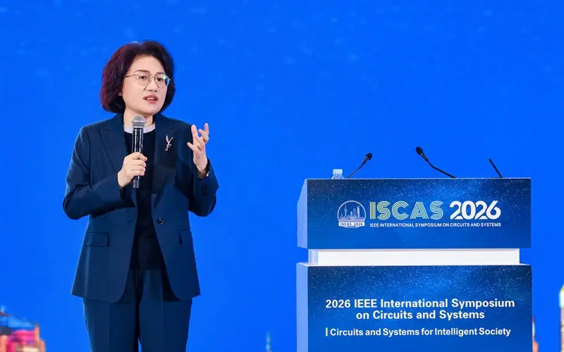
At the 2026 IEEE International Symposium on Circuits and Systems (ISCAS), He Tingbo, a senior executive at Huawei, officially unveiled the Tau (τ) Scaling Law. The framework proposes a profound shift in microchip architecture: moving the primary target of semiconductor optimization away from geometric transistor size (nanometers) and directly toward signal speed (time).
What is the Tau (τ) Scaling Law?
In classic circuit theory, the Greek letter Tau (τ) represents a time constant—the measurement of how quickly an electrical signal can toggle from one state to another without being degraded by resistance and capacitance (known as RC delay). The smaller the τ, the faster and more energy-efficient the chip becomes.
For decades, the tech sector relied on Moore’s Law, which focused heavily on shrinking physical transistors to pack more of them onto a two-dimensional silicon wafer. Huawei’s Tau Scaling Law turns this focus on its head. Instead of simply packing more “workers” onto a factory floor, it reorganizes the layout of the entire factory to shorten the distance data needs to travel.
To achieve this, Huawei introduced a proprietary structural technology called LogicFolding. By breaking through traditional 2D layout constraints and folding circuits into 3D configurations, the technology radically shortens critical wiring paths, boosting density and performance without relying exclusively on the world’s most advanced, heavily restricted lithography nodes.

Industry Commentary: A Strategic Game Changer
The tech world has reacted with immense interest to the framework, viewing it as a sophisticated system-level alternative while a post-Moore’s Law standard remains elusive.
Tian Feng, the director of the Kuaisi Manxiang Research Institute, framed the presentation as a definitive pivot in global tech competition:
“Huawei has redefined the yardstick of performance evolution, shifting the goal from transistor size to signal delay. This changes the game from a single track of process chasing to a dual track of process plus system innovation.”
Tian further argued that measuring tech progress purely by nanometers is becoming an incomplete metric due to skyrocketing lithography costs and extreme physical limitations.
Expressing an academic perspective, Hu Yanping, a professor at the Digital Frontier Research Institute at the Shanghai University of Finance and Economics, emphasized that the artificial intelligence boom makes this pivot necessary:
“Explosive computing demand requires someone to send the turn signal. It is encouraging that companies are beginning to move beyond path dependency and explore new paradigms, even if the ultimate test will remain real-world validation.”

Proven Traction and the 1.4nm Horizon
While critics initially questioned whether the Tau Law was purely theoretical, Huawei revealed that the methodology has been quietly operating under real-world conditions for years. The company confirmed it has designed and mass-produced 381 distinct chip models using this exact design ethos over the past six years.
Looking forward, Huawei projects that this architectural blueprint will allow its high-end chips to achieve transistor densities equivalent to a 1.4-nanometer-class process by 2031, bypassing the immediate need for next-generation lithography equipment.
Zhang Lixing, chairman of Wuxi Chipown Micro, simplified the engineering shift using a manufacturing analogy:
“Moore’s Law is like putting more workers on a production line. The Tau Law is about speeding up the turnover of parts on that line. It optimizes data transmission efficiency across the stack… the core metric is the reduction of signal transfer time.”
The Challenges Ahead
Despite the optimism, experts note that scaling the Tau framework globally requires a robust software ecosystem, particularly in system-level Electronic Design Automation (EDA) tools. Cang Wei, vice president of Xpeedic Technology, noted:
“The Tau Law provides one ruler for process engineers, architects, and system designers to collaborate. But for this to benefit the entire industry, we must strengthen domestic capabilities in system-level EDA to support this new paradigm.”
Recognizing the immense collaborative effort required to institutionalize this blueprint, Huawei’s He Tingbo concluded her presentation with an open call to the global scientific community, noting: “No single company can independently find all the answers.”
Source: CGTN